RESEARCH
Active Voltage Balancing Embedded Digital Gate Driver for Series-Connected 10 kV SiC MOSFETs

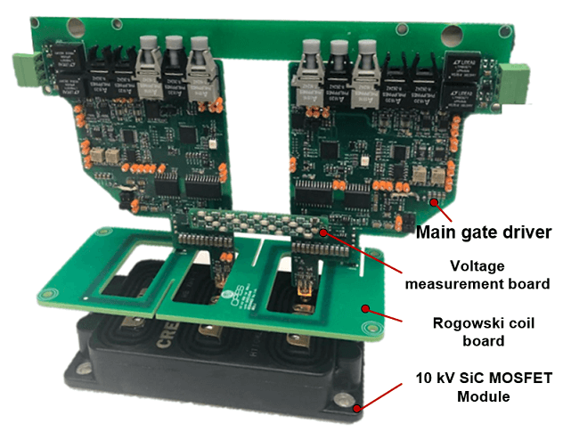
For this purpose, a new gate driver (shown in Fig. 1) is designed for active voltage balancing of two series-connected 10 kV SiC MOSFETs. The basic driving features of the gate driver design in- cludes the high common-mode (CM) noise rejection layout, an active Miller clamp circuit and Rogowski switching current sensor-based fault protection. An FPGA is implemented for each device to coordinate the switching timing, protection, and active balancing logic. To achieve active voltage balancing, the following features are also designed: 1) miniaturized 10 kV drain-source voltage measurement unit and its interconnection to gate-driver; 2) tunable gate signal de- lay time adjustment unit with 0.25 ns resolution; and 3) Rogowski current sensing unit for fault current detection.
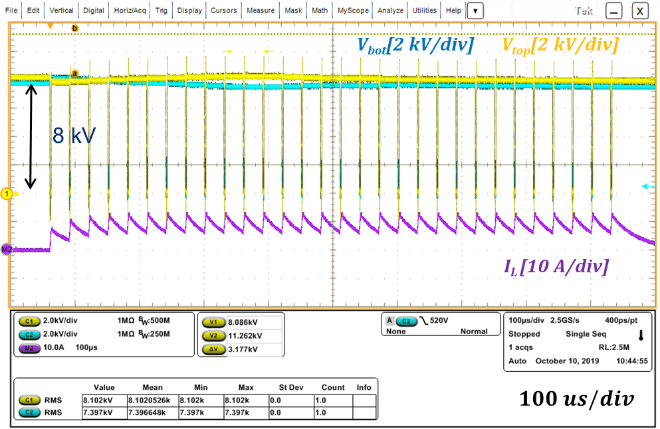
Based on the developed gate driver, the FPGA-based closed- loop gate signal timing control for active voltage balancing of se- ries-connected 10 kV SiC MOSFETs is designed. In each switching cycle, the gate driver of the bottom device imposes an additional de- lay time to the falling edge of the gate signal to control the turn-off time difference between the series-connected devices. The regulator is designed to adjust the delay time with a fixed-time step in each switching cycle. In order to have the capability to increase or reduce the bottom device voltage, a constant delay time is applied to the top gate driver so the bi-directional adjustment of turn-off time can be readily achieved. For protection, the gate driver of series-connected 10 kV SiC MOSFETs detect fault separately. When the overcurrent or short-circuit fault happens, each gate driver sends the fault signal to the main controller and lets the main controller shut down the gate signals for series-connected devices simultaneously. The normal turn-off instead of soft turn-off is applied in such a protection strat- egy.The proposed gate driver and active voltage balancing method are validated in a phase-leg test achieving 16 kV total blocking volt- age, as shown in Fig. 2.


